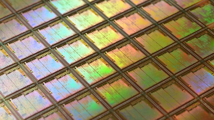
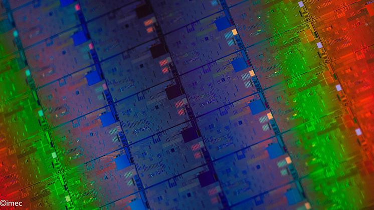
Wafer-scale production of graphene-based photonic devices
Graphene Flagship researchers have devised a wafer-scale fabrication method that paves the way to the next generation of telecom and datacom devices.
Graphene Flagship researchers have devised a wafer-scale fabrication method that paves the way to the next generation of telecom and datacom devices.
Funded by the European Commission, this €20 million project will enable large volume production of electronic devices based on two-dimensional materials.
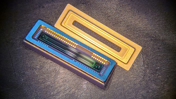
Graphene Flagship partner, Emberion, is launching a new wide spectrum graphene photodetector at Laser World of Photonics on June 24 to 27 Munich, Germany. Showcased in Hall A2 at stand 113/3, the linear array can enable on-site analysis of food and agriculture products using infrared detection — at a lower cost than existing indium gallium arsenide infrared sensors.
Bringing together 118 academic and industrial partners in 12 research and innovation projects and 1 coordination and support project, the Graphene Flagship initiative will continue to advance Europe’s strategic autonomy in technologies that rely on graphene and other 2D materials. The initiative, which builds on the previous 10-years of the Graphene Flagship, is funded by the European Commission’s Horizon Europe research and innovation programme. The 2D-Experimental Pilot Line, addressing the challenges of upscaling 2D material production processes for the semiconductor industry, is another key component of the Graphene Flagship ecosystem.